Monolithic Active Pixel Sensors (MAPS) in a Quadruple Well Technology for Nearly 100% Fill Factor and Full CMOS Pixels
Jamie Alexander Ballin, Jamie Phillip Crooks, Paul Dominic Dauncey, Anne-Marie Magnan, Yoshinari Mikami, Owen Daniel Miller, Matthew Noy, Vladimir Rajovic, Marcel Stanitzki, Konstantin Stefanov, Renato Turchetta, Mike Tyndel, Enrico Giulio Villani, Nigel Keith Watson, John Allan Wilson
Abstract
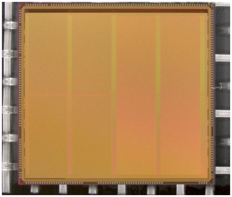
'Anne-Marie Magnan' 'Yoshinari Mikami' 'Owen Daniel Miller' 'Matthew Noy' 'Vladimir Rajovic' 'Marcel Stanitzki' 'Konstantin Stefanov' 'Renato Turchetta' 'Mike Tyndel' 'Enrico Giulio Villani' 'Nigel Keith Watson' 'John Allan Wilson'] In this paper we present a novel, quadruple well process developed in a modern 0.18 μm CMOS technology called INMAPS. On top of the standard process, we have added a deep P implant that can be used to form a deep P-well and provide screening of N-wells from the P-doped epitaxial layer. This prevents the collection of radiation-induced charge by unrelated N-wells, typically ones where PMOS transistors are integrated. The design of a sensor specifically tailored to a particle physics experiment is presented, where each 50 μm pixel has over 150 PMOS and NMOS transistors. The sensor has been fabricated in the INMAPS process and first experimental evidence of the effectiveness of this process on charge collection is presented, showing a significant improvement in efficiency.
§ The Valyu brief
Reading the full paper and taking notes. This takes a few seconds…
§ Ask this paper
Ask a question about this paper
Valyu reads the full text and answers from what the paper actually says.
Searching the other archives…